BSP 296
SIPMOS ® Small-Signal Transistor
• N channel
• Enhancement mode
• Logic Level
• VGS(th) = 0.8...2.0V
Pin 1
G
Pin 2
Pin 3
D
Type
VDS
ID
RDS(on)
Package
Marking
BSP 296
100 V
1A
0.8 Ω
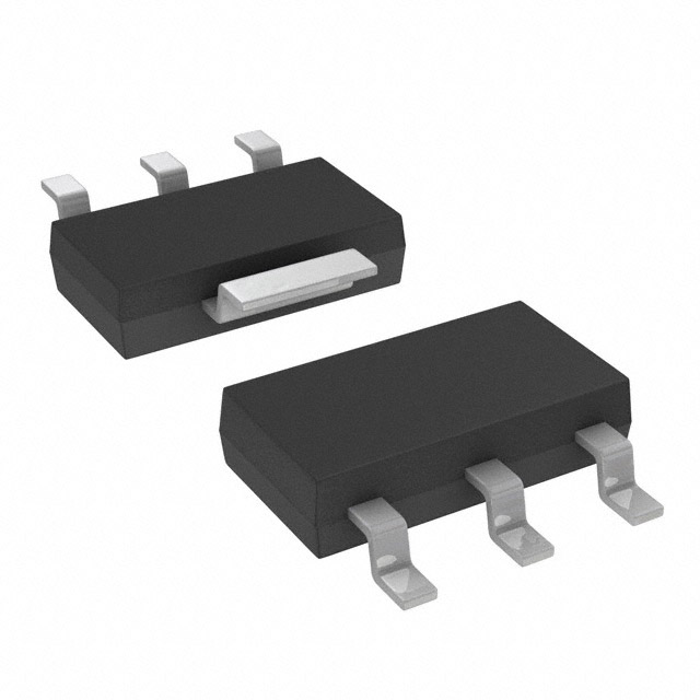
SOT-223
BSP 296
Type
BSP 296
Ordering Code
Q67000-S067
Pin 4
S
D
Tape and Reel Information
E6327
Maximum Ratings
Parameter
Symbol
Drain source voltage
VDS
Drain-gate voltage
V
100
Unit
V
DGR
RGS = 20 kΩ
100
Gate source voltage
VGS
ESD Sensitivity (HBM) as per MIL-STD 883
± 20
Class 1
Continuous drain current
A
ID
TA = 42 ˚C
1
DC drain current, pulsed
IDpuls
TA = 25 ˚C
4
Power dissipation
W
Ptot
TA = 25 ˚C
Data Sheet
Values
1.8
1
05.99
�BSP 296
Maximum Ratings
Parameter
Symbol
Chip or operating temperature
Tj
-55 ... + 150
Storage temperature
Tstg
-55 ... + 150
Thermal resistance, chip to ambient air
RthJA
≤ 70
R thJS
≤ 10
Thermal resistance, junction-soldering point
1)
Values
DIN humidity category, DIN 40 040
Unit
˚C
K/W
E
IEC climatic category, DIN IEC 68-1
55 / 150 / 56
1) Transistor on epoxy pcb 40 mm x 40 mm x 1,5 mm with 6 cm2 copper area for drain connection
Electrical Characteristics, at Tj = 25˚C, unless otherwise specified
Parameter
Symbol
Values
min.
typ.
Unit
max.
Static Characteristics
Drain- source breakdown voltage
V
V (BR)DSS
VGS = 0 V, ID = 0.25 mA, Tj = 25 ˚C
100
-
-
0.8
1.4
2
VDS = 100 V, V GS = 0 V, Tj = 25 ˚C
-
0.1
1
VDS = 100 V, V GS = 0 V, Tj = 125 ˚C
-
8
50
VDS = 60 V, VGS = 0 V, Tj = 25 ˚C
-
-
100
Gate threshold voltage
V GS(th)
VGS=VDS, ID = 1 mA
Zero gate voltage drain current
Gate-source leakage current
IDSS
Drain-Source on-state resistance
-
10
100
Ω
RDS(on)
VGS = 10 V, ID = 1 A
-
0.55
0.8
VGS = 4.5 V, ID = 1 A
-
0.95
1.4
Data Sheet
2
nA
nA
IGSS
VGS = 20 V, VDS = 0 V
µA
05.99
�BSP 296
Electrical Characteristics, at Tj = 25˚C, unless otherwise specified
Parameter
Symbol
Values
min.
typ.
Unit
max.
Dynamic Characteristics
Transconductance
S
gfs
VDS≥ 2 * ID * RDS(on)max, ID = 1 A
Input capacitance
0.5
-
300
400
-
60
90
-
30
45
Crss
VGS = 0 V, V DS = 25 V, f = 1 MHz
Turn-on delay time
pF
Coss
VGS = 0 V, V DS = 25 V, f = 1 MHz
Reverse transfer capacitance
-
Ciss
VGS = 0 V, V DS = 25 V, f = 1 MHz
Output capacitance
1.3
ns
td(on)
VDD = 30 V, VGS = 10 V, ID = 0.29 A
RGS = 50 Ω
Rise time
-
8
12
-
15
25
-
120
160
-
65
85
tr
VDD = 30 V, VGS = 10 V, ID = 0.29 A
RGS = 50 Ω
Turn-off delay time
td(off)
VDD = 30 V, VGS = 10 V, ID = 0.29 A
RGS = 50 Ω
Fall time
tf
VDD = 30 V, VGS = 10 V, ID = 0.29 A
RGS = 50 Ω
Data Sheet
3
05.99
�BSP 296
Electrical Characteristics, at Tj = 25˚C, unless otherwise specified
Parameter
Symbol
Values
min.
typ.
Unit
max.
Reverse Diode
Inverse diode continuous forward current
A
IS
TA = 25 ˚C
Inverse diode direct current,pulsed
1
-
-
4
V
V SD
VGS = 0 V, IF = 2 A, Tj = 25 ˚C
Data Sheet
-
ISM
TA = 25 ˚C
Inverse diode forward voltage
-
-
4
0.95
1.3
05.99
�BSP 296
Power dissipation
Ptot = ƒ(TA)
Ptot
Drain current
ID = ƒ(TA)
parameter: VGS ≥ 10 V
2.0
1.1
W
A
1.6
ID
0.9
0.8
1.4
0.7
1.2
0.6
1.0
0.5
0.8
0.4
0.6
0.3
0.4
0.2
0.2
0.1
0.0
0.0
0
20
40
60
80
100
120
˚C
160
0
20
40
60
80
100
TA
120
˚C
160
TA
Safe operating area ID=f(VDS)
Transient thermal impedance
Zth JA = ƒ(tp )
parameter: D = tp / T
parameter : D = 0, TC=25˚C
10 2
K/W
10 1
ZthJA
10 0
10 -1
D = 0.50
0.20
10 -2
0.10
0.05
10 -3
single pulse
0.02
0.01
10 -4
-8
-7
-6
-5
-4
-3
-2
-1
0
10
10
10
10
10
10
10
10 s 10
tp
Data Sheet
5
05.99
�BSP 296
Typ. output characteristics
ID = ƒ(VDS)
parameter: tp = 80 µs , Tj = 25 ˚C
2.4
Typ. drain-source on-resistance
RDS (on) = ƒ(ID)
parameter: tp = 80 µs, Tj = 25 ˚C
2.6
Ptot = 2W
l
j
k
ihgf
A
Ω
e
d
1.8
1.6
1.4
c
1.2
1.0
0.8
0.6
b
2.5
c
3.0
d
3.5
e
4.0
f
4.5
g
5.0
h
6.0
i
7.0
j
8.0
b k
9.0
l
10.0
RDS (on)
2.0
1.8
1.6
1.4
1.2
1.0
c
0.8
d
ihgf j
ke
0.6
0.4
0.4
a
0.2
b
2.2
VGS [V]
a
2.0
2.0
ID
a
VGS [V] =
0.2
0.0
a
2.5
2.0
b
3.0
c
3.5
d
4.0
e
f
4.5 5.0
g
6.0
h
i
7.0 8.0
j
9.0
0.0
0.0 0.5 1.0 1.5 2.0 2.5 3.0 3.5 4.0
V
5.0
0.0
0.2
0.4
0.6
0.8
1.0
1.2
VDS
A
1.5
ID
Typ. transfer characteristics ID = f(V GS)
Typ. forward transconductance gfs = f (ID)
parameter: tp = 80 µs
parameter: tp = 80 µs,
ID
k
10.0
4.5
2.0
A
S
gfs
3.5
1.6
1.4
3.0
1.2
2.5
1.0
2.0
0.8
1.5
0.6
1.0
0.4
0.5
0.2
0.0
0.0
0
1
2
3
4
5
6
7
8
V
10
0.0
VGS
Data Sheet
0.5
1.0
1.5
2.0
2.5
3.0
A
4.0
ID
6
05.99
�BSP 296
Drain-source on-resistance
RDS (on) = ƒ(Tj )
parameter: ID = 1 A, VGS = 10 V
Gate threshold voltage
VGS (th) = ƒ(Tj )
parameter: VGS = VDS, ID = 1 mA
2.0
4.6
Ω
V
4.0
RDS (on) 1.6
VGS(th)
1.4
3.6
3.2
1.2
2.8
2.4
98%
1.0
98%
2.0
0.8
typ
typ
1.6
0.6
1.2
2%
0.4
0.8
0.2
0.4
0.0
0.0
-60
-20
20
60
100
˚C
160
-60
-20
20
60
100
˚C
Tj
160
Tj
Typ. capacitances
Forward characteristics of reverse diode
IF = ƒ(VSD)
parameter: Tj , tp = 80 µs
C = f (VDS)
parameter:VGS=0V, f = 1 MHz
10 3
10 1
pF
A
Ciss
C
IF
10 2
10 0
Coss
Crss
10 1
10 -1
Tj = 25 ˚C typ
Tj = 150 ˚C typ
Tj = 25 ˚C (98%)
Tj = 150 ˚C (98%)
10 0
0
5
10
15
20
25
30
V
10 -2
0.0
40
VDS
Data Sheet
0.4
0.8
1.2
1.6
2.0
2.4
V
3.0
VSD
7
05.99
�BSP 296
Safe operating area ID=f(V DS)
Drain-source breakdown voltage
V(BR)DSS = ƒ(Tj)
parameter : D = 0.01, TC=25˚C
120
V
116
V(BR)DSS114
112
110
108
106
104
102
100
98
96
94
92
90
-60
-20
20
60
100
˚C
160
Tj
Data Sheet
8
05.99
�


 工商网监
湘ICP备2023018690号
工商网监
湘ICP备2023018690号
